|
|
|
|
|
|
by GlibMonkeyDeath
66 days ago
|
|
|
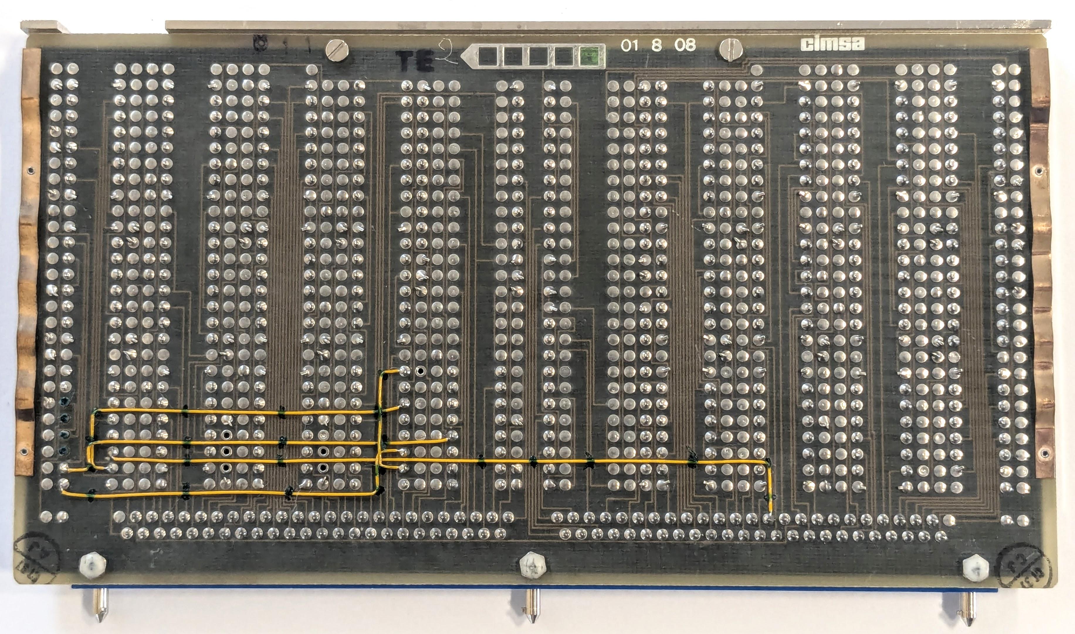
The PCB construction is curious (which you say is multi-layer) - why use a grid of 0.1" holes? Is that so it could be easily jumpered? Can you tell if the traces run through the holes or between them? I don't have the patience to reverse-engineer these types of boards, but I do find them really interesting to think about. CAD was just getting started (I just looked up that Gerber format was released in 1980) so I wonder if the masks were hand-drawn. |
|
|