|
|
|
|
|
|
by mbitsnbites
882 days ago
|
|
|
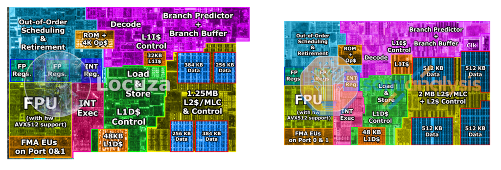
I'll have to read up on Agner's findings. My assumptions are largely based on annotated die shots, like this one of Rocket Lake (IIRC): https://substackcdn.com/image/fetch/f_auto,q_auto:good,fl_pr... If they are correct, the uOP cache consumes at least as much silicon as the L1I cache, while they generally can hold fewer instructions. Some napkin math: x86 instructions are 4 bytes long on average, so a 32KiB L1I can hold 32/4=8K instructions, while the uOP cache can hold 4K uOP instructions (how many uOPs does an x86 instruction translate to on average?). That would indicate that uOP:s require twice the silicon area to store compared to "raw" x86 instructions - or that the uOP cache is more advanced/complex than the L1I cache (which may very well be the case). Also visible from the die shots: decoding and branch prediction are far from free. |
|
|
So really depends on what the balance is. If it was two or three of those memory cell blocks, I agree it's quite big. But if it's just one, it's actually quite small.
Agner's findings are for the Sandybridge implementation. He says Haswell and Skylake share the same limitations, but doesn't look like he has done much research into the later implementations.
The findings actually point to the uOP cache being much simpler in structure. The instruction cache has to support arbitrary instruction alignment and fetches that cross boundaries. The uOP cache has strict alignment requirements, it delivers one cache line per cycle and always delivers the entire line. If there aren't enough uops, then the rest of the cacheline is unused.
> Also visible from the die shots: decoding and branch prediction are far from free.
Yeah, it appears to be massive. And I get the impression that block is more branch prediction than decoding.
Nothing is free in CPU design, it's just a massive balancing act.