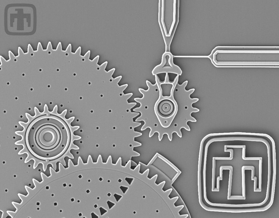
| Good overview, but he's missing one of the coolest applications of semiconductor / photolithography. MEMS. Micro-electromagnetic systems. The most common MEMS I can think of is the comb sensor, used for accelerometers in all of your cell phones. https://www.memsjournal.com/2010/12/motion-sensing-in-the-ip... The MEMS sensor for an accelerometer is quite simple. Take the nearest comb and smack it against a desk: you'll notice that the comb vibrates in one direction. Now hook up two combs and interleave their teeth together so that they're barely touching. When they touch, an electrical signal is sent through them to sense when they touch. Add differently sized teeth, the larger the spacing the more acceleration is needed before they activate. (EDIT: Looks like the iPhone MEMS uses capacitance... similar concept though, the capacitance changes based off of how far away these teeth are from each other and you can measure that using college-level electronics) Finally, have these teeth rotated in all directions, so that you can sense all the directions in one little device. -------- MEMS are about using the physical properties of object, but just making these small physical objects really, really, really tiny thanks to the magic of photolithography. You can see this literal comb structure by looking at any accelerometer under a microscope: https://memsjournal.typepad.com/.a/6a00d8345225f869e20148c70... ------ If the accelerometer is too difficult for you to understand, the "beginner MEMS" is gears. https://www.sandia.gov/app/uploads/sites/145/2021/11/1-1.jpg You can make any shape you want with modern chip-making tools. The "shape" most people want is a transistor (gate, drain, source). But in many ways, a teeny-tiny gear is simpler to think about. The practical applications of micro-scale MEMS (gears, combs, springs, etc. etc. ) is somehow harder to think about than computers, so there aren't very many practical MEMS around. But still, practical MEMS help remind us that all of these chip-making tools exist in the real, physical world. Albeit at a very small scale. |