I am a KiCad user, should I switch to Horizon and why?
From the docs it seems like your main selling point is a better library, why not just make a better library for KiCad?
Back-annotation and library management are the two places where KiCad really falls down for me (the user interface is janky but works once you get used to the warts) so this looks really interesting.
How tightly integrated are the schematic editor and layout editor? Are they two separate programs like KiCad or can you eg. delete a component from the schematic and have it automatically removed from the PCB (but without nuking ALL non-schematic components from the PCB).
You have to click a "Update netlist" Button first otherwise this won't happen. However if you select something in the schematic editor, the selection is highlighted in the board view and vice versa.
I only got to know about LibrePCB at the end of 2016 after several months of development on Horizon EDA. While there are some similarities such as the use of UUIDs and strong link between schematic and netlist, there are major architectural differences such as Horizon EDA using raw OpenGL vs QTSceneGraph(?) and Gtkmm vs QT.
As far as I can tell, the development models also differ significantly: The LibrePCB devs seem to be focused on doing things the right way the first time such as having a proper operation-based undo/redo stack whereas horizon just stores a copy of the whole schematic/board for undo/redo. They also seem to focus more on simplicity for beginners rather than more advanced features such as length tuning and advanced design rules.
Putting development effort where I like enabled me do to the board for my master thesis https://github.com/carrotIndustries/x-band-tx/ (4 Layers, differential pairs, length-matched traces) in Horizon EDA only after about 2 years after the initial beginning of development.
I still remember introducing you to Urban, the main LibrePCB developer, at FOSDEM after meeting you at 33c3 (was it 33c3?) the same year. It was fun listening to the two of you talking about your design decisions, where you came up with almost identical solutions (UUIDs for library elements for example) and where you went different paths.
We also talked about ways to increase collaboration between the two tools. A few ways I could see is:
* Router: Extracting the KiCad router into a separate repository / library so it can be used and developed by the different projects.
* Gerber Compatible Stroke fonts: Would be nice to have one font specification and implementation to be used for PCBs. LibrePCB started the FontoBene (https://github.com/fontobene) project to do just this, but currently LibrePCB is the only user of it.
* Regular exchange of ideas and domain specific problems / challenges and solutions. This already happened a few times at c3 and FOSDEM.
1. Yes it does, has even a Annotation mode to add sheet increments for part numbers (e.g. R101, R102, etc for the first sheet, R201, R202, etc for the second sheet). Pasting between sheets works, having multiple gatesn (e.g. of a hex inverter) spread out over multiple sheets works as well.
2. yes, including global or per-net rules for thermal relief, spacing etc. It warns you if nets have not been recalculated on Fabrication output. Adding them is simply: draw a polygon, right-click and "Add Plane", there you have to select any names net.
3. there is length tuning built in, but quite frankly I never had to use it, so I don't know if that is what you're looking for
re 1 and 2: awesome! I'm excited and will be trying out Horizon my next design.
re 3: I was more thinking about the plane spacing. Like say I'm making a board where I want to carry a high-speed clock signal. If it's single-ended, chances are the transmitter has a 50-ohm output impedance, and the receiver has a 50-ohm input impedance.To get the cleanest signal, I want my trace to have a 50-ohm _characteristic_ impedance (which is a function of the trace-width, distance to the closest plane layer, and PCB substrate's chemical properties).
Trying to model it accurately is a huge pain in the ass, and probably not worth attempting. But it could be nice to have a rule-checker that says something like "for your PCB dielectric constant of 4.7 with 10mil spacing to the nearest plane, your trace should be 18mil wide to get the desired impedance".
There are a bunch of these calculators out there - but it would be super cool to do some rudimentary constraints as DRC!
1. Does Horizon support an equivalent to the 'Variant Manager?' This is something that will allow variance of build outputs (different component populations, different schematic text, etc).
2. In the docs it seems to mention submitting parts to the default pool. If people submit parts to the pool are there style guides somewhere? (line widths, US vs EU resistor symbols, etc)
3. Looking at a random SMD footprint (SOT-363) it looks like the paste window is equal to the pads. Is there a way to set paste mask expansion like is done in Altium? (Automatically offset paste window from pad by some amount)
    1. Opening up your first project is not straightforward. Instead of just opening with a blank project and letting you add a resistor, the app asks a lot of rather irritating and irrelevant questions (who cares who the "author" is at creation time, and couldn't it guess anyways?) that could be better decided later. Worst offense: the "create" button is grayed. As in: nope, you won't be able to use me until you answer all the useless trivia.

    2. Horizon seems to cling to the "main window launches sub-apps" paradigm (much like kicad). This is a rather confusing UX workflow. At the very least, it clutters up your desktop. Why can't all sub-app live under one roof ? I mean even gimp has finally given up on the broken multiple top window idea ages ago.

    3. Couldn't find any standard old-timey thru-hole parts in the default "pool": 2N2222, 2N3904 standard, LEDs. Not fashionable these days for serious work, but still very much in demand by the hobby crowd.

    4. To place a part, it looks like you have to select the *exact* component you need right away. Why? . Why can't I just place a generic NPN in the diagram and then refine what part it'll actually be later on ?

    5. The part browser : why so many search boxes ? I want a Google-style single search box that's smart enough to match what I'm saying to a given part. Finding a part shouldn't be like entering an SQL statement. Fuzzy matcher please.

    6. Right-click on a component: a mile long menu, no "part properties" entry. When I finally locate the "change symbol" entry (in a sub-menu), it sends you to a subtly different UI than the part browser.

    7. No navigation buttons in sight. Where's "Frame All", "Frame component"

    8. Components are hard (near impossible) to just grab-and-move
I'll have to play with it more, but the initial interaction with the UX is kinda icky.
[edit]: forgot to mention installation. On ubuntu, this was not exactly straightforward. Choice between installing a binary through flatpak (non-standard thing I don't have) or building from scratch (there went 30mn of my day). Almost made me open the windows laptop that's specifically reserved for running win-only crapware.
- on 1: Starting projects: for me it is only entering a project title and selecting a path, which is reasonable unless you are the type who wants to decide things like these in the end on saving.
- on 2: While I also like single window concepts better (with panes like Blender), I think having schematic, board and pool/library editors in seperate windows is kinda reasonable.
- on 4: You actually can. You are not forced to use existing parts if you use "Place component"
- on 6: Given how the whole thing works, such a thing like "Part properties" doesn't really make sense. In Horizon everything you place on the schematic is either a generic unit (E.g. "Two-terminal resistor") where you can enter a value or a existing part mapped to this generic unit (e.g. a "ERJ-6ENF2003"). This is (on purpose) different from how other EDA-tools do it, but in practise it works quite well. The point on the different assign window is something I'd like to have changed as well : )
- on 8: if you want to move something you have to use the move tool which you invoke by pressing the m key. You can also move things with the arrow keys.
Generally the UX paradigm of horizon is very much built around single key shortcuts or key sequences. And if you don't know the keys just press the spacebar and search for the command and it will tell you right there.
As for now the experience for power users is very fluid, but when it comes to installation, onboarding etc. the whole thing could use a lot of improvement (and are gladly beeing worked on).
Gtk's and horizon's OpenGL requirements (3.3 core profile + extensions) likely aren't met by whatever graphics adapter your VM implementation provides.
that helps, I checked and Parallels 15 only supports OpenGL 3.2. I think it would be a good idea to maybe improve the error message, or put a check in the installer.
Thanks for your work, as it currently stands I can't use it but I appreciate it exists nonetheless (I'm on a Mac).
It is, but I also understand where the author is coming from. OpenGL 3.2/3.3 with the introduction of the Core Profile is where I remember the OpenGL API getting seriously more ergonomic - no screwing around with GLEW to load extensions for basic functionality, etc.
Similarly, gtkmm is so much cleaner than Qt as a modern C++ library with none of the preprocessor / codegen quirks. Unfortunately it limits the platform reach, because GTK isn't really polished anywhere except Linux.
I raise a toast to the obsession with clean code and clean design. Sometimes "works on my machine" is the counter to "worse is better." At the same time, it's pretty inconvenient for me to use the software. Oh well.
Nice work! The world badly needs a FOSS EDA program that isn't insane.
Any plans for Mac downloads? And also, does its component model separate out schematic symbols and pin assignment (like DesignSpark PCB and I assume others) or are they inseparable (like KicadPCB)?
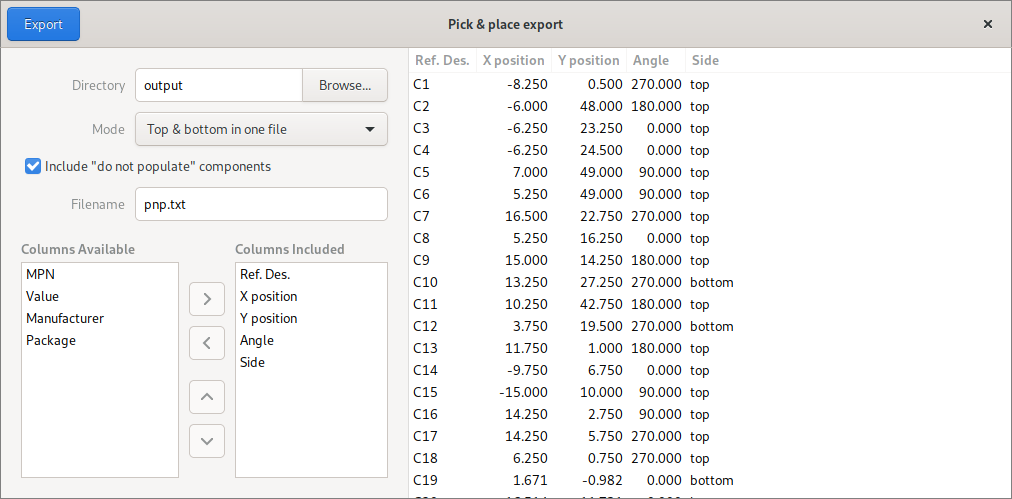
When producing a placement file for a PCB, can component part numbers be exported ? Neither Cadence, nor KiCAD stores components in their PCB files, only footprints, so part numbers cannot be easily accessed.
I wish they had git or something built into KiCad, specially to update parts and be able to find libraries, instead having to search for them online and downloading and extracting and adding to two places in the software.
They sort of do, the official KiCAD part libraries are actually hosted on Github https://kicad.github.io/. A lot of distributions kinda mess this up by distributing static snapshots, but I usually clone the Git repo and then direct KiCAD to that. The base libraries cover a ton of parts, and I then keep all my self-drawn or individually downloaded parts in a separate library.
It's still a pretty clunky workflow but it gets the job done. I really wish it was possible to have a point and click interface in the GUI for downloading individual new parts akin to a Linux package manager, but this is probably difficult to manage since there is no centralized distribution point for parts that are outside of the official libraries.