|
|
|
|
|
|
by Dylan16807
3666 days ago
|
|
|
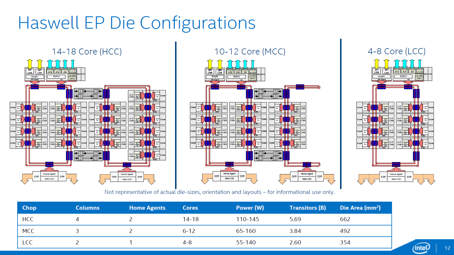
> The chip has to be small enough that the clock can propagate everywhere within the chip within a single cycle, or problems will occur. Problems like what? These chips are already chopped up into different clock domains, and it's easy to install some PLLs so that perfectly-synchronized clock signals can blanket a chip even if it's inches across. Moving data around is also not a big deal. The Xeons in the article already have multi-nanosecond ring busses running around between cores[1]. They don't slow the chip down because the design simply lets long-distance data transfers take multiple cycles. L3 and I/O don't have to be blazingly fast in terms of latency. [1] http://images.anandtech.com/doci/8423/HaswellEP_DieConfig.pn... |
|
|
The chip won't work.
> These chips are already chopped up into different clock domains, and it's easy to install some PLLs so that perfectly-synchronized clock signals can blanket a chip even if it's inches across.
Sorry, I didn't explain myself well enough. Of course chips have different clock domains, but these also come at a cost. The more synchronization you need to do between domains, the less die space you have for computationally useful stuff.
> L3 and I/O don't have to be blazingly fast in terms of latency.
I would argue differently, the impact of latency is highly dependent on the type of computation you're doing. If you're doing something with a lot of data (say, encoding video) then you need to be moving data as quickly as possible between the processor and memory. Any additional latency in cache or I/O will cause the performance to suffer.
Ideally, you want the latency of L3 and I/O to be as low as possible.